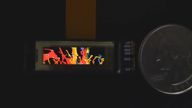
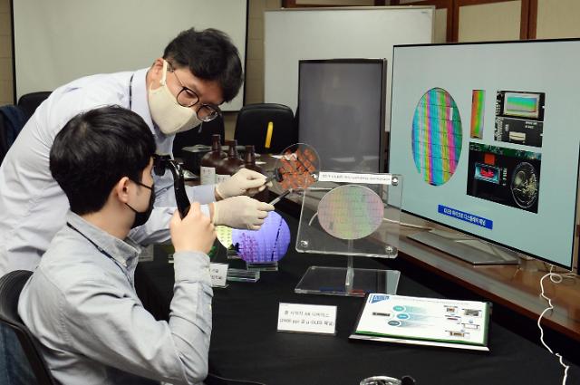
[Courtesy of ETRI]
SEOUL -- For the first time in the world, researchers from a state research institute have succeeded in the development and commercialization of new photoresist material that can be cured at a low temperature. A prototype high-definition organic light-emitting diode display was produced using the photoresist material.
A photoresist is a light-sensitive material mainly used in the production of liquid crystal display (LCD) and organic light-emitting diode (OLED) display panels. South Korean companies, which create the world's top-class display panels, have been heavily dependent on foreign photoresist materials. More than 90 percent of photoresists and fluorine polyimide and 44 percent of etching gas, a vital chemical used in the production of semiconductors, used to come from Japan, according to the Korea International Trade Association.
South Korean semiconductor and display companies were put to an unexpected stalemate when Tokyo imposed trade restrictions in 2019 on key materials for electronic parts and products. The move was regarded as Tokyo's retaliatory action over a decision by South Korea's highest court in October 2018 that acknowledged individual rights to get compensation for wartime forced labor.
Instead of negotiating with Tokyo, Seoul chose to accelerate the localization of key materials and decided to inject six trillion won ($5 billion) for six years to reduce the technological gap with Japan and diversify and enhance the production of materials and parts.
Of key materials and components brought in from Japan, photoresists were one of the hardest to localize as they require top-notch techniques that involve high temperature and high pressure. While the high-temperature production method had no problem with LCD panels with a layer of glass that can withstand heat, OLEDs were easily damaged by the heat created during the production process.
[Courtesy of ETRI]
Using localized materials, researchers were able to produce a 0.7-inch OLED display prototype, the institute said in a statement on November 9. The high-definition display had 2,300 pixels that are smaller than three micrometers. The display was commercialized through an exclusive supply deal with an undisclosed company.
"Through collaboration between the government, corporates and a state research institute, we were able to localize core materials," ETRI head researcher Cho Nam-sung was quoted as saying. The institute would upgrade its technology to put more than 3,000 pixels into a 0.7-inch display.
reporter

Park Sae-jin
swatchsjp@ajunews.com
![[CES2024] LG Electronics to showcase wireless transparent OLED TV for first time at CES](https://image.ajunews.com/content/image/2024/01/08/20240108155434102725.jpg)