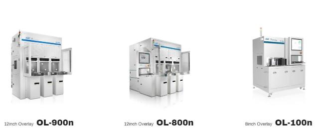
[Courtesy of Auros Technology]
Auros, which specializes in overlay measurement equipment, showed a steep rise from the public offering price of 21,000 won to trade at the daily limit of 54,600 won soon after the market opened on February 24. Investors gave a positive assessment of Auros' growth potential after CEO Lee Jun-woo promised to expand the company's global market share from 5 percent to 15 percent by 2023.
"We will lay the groundwork for growing into a competitive measurement inspection company in the global market by utilizing investments through public offerings," Lee said in a pre-IPO session. Auros is the only South Korean company that has acquires original technology in overlay measuring equipment. The main client is SK hynix, a major microchip producer in South Korea.
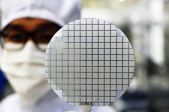
Wafers go through a repeated process of stamping patterns, covering with materials, cutting, and washing. An overlay measuring equipment checks whether materials are correctly aligned on the top of the wafers. It applies a ray of light to the wafer and analyzes the reflected light to detect errors in nanometers and correct the location of lithography equipment.
Auros has also developed a metrology system that can accurately measure the alignments between very tiny pads and bumps of different sizes in the wafer-level packaging. FST, the only domestic provider of pellicles, owns 42.5 percent of Auros. A pellicle is a thin membrane stretched over an aluminum frame and glued to the photomask to protect it from contaminants. Even if particles sit on the membrane, they are not printed on the wafer because they are out of focus during the exposure from the lithography process.
reporter

Lim Chang-won
cwlim34@ajunews.com